


The global semiconductor industry has entered an era of unprecedented strategic importance and capital reinvestment. Driven by geopolitical mandates, sovereign supply chain reshoring initiatives like the U.S. CHIPS and Science Act, and the exponential computing demands of Artificial Intelligence and autonomous systems, the race to build domestic manufacturing capacity has reached a fever pitch. Multi-billion-dollar “mega-fabs” are rising across the United States and Europe, while established foundries and Integrated Device Manufacturers (IDMs) push the boundaries of physics toward sub-2nm process nodes and advanced 3D packaging.
However, the industry faces an existential operational bottleneck that cannot be solved by capital expenditures alone: a profound, global deficit of experienced semiconductor executive talent. Constructing a state-of-the-art cleanroom and ordering multi-million-dollar extreme ultraviolet (EUV) lithography systems is only half the battle. Without battle-tested executives—leaders who have successfully navigated high-volume manufacturing (HVM) ramps, mitigated nanometer-level yield disasters, managed complex cleanroom labor ecosystems, and balanced massive CapEx budgets—these multi-billion-dollar investments sit idle or bleed capital.
For corporate boards, venture sponsors, and CEOs across both commercial foundries and fabless semiconductor companies venturing into custom silicon, hiring the right operations and engineering executives is a make-or-break endeavor. The talent pool is exceedingly narrow, fiercely defended, and highly specialized. This comprehensive executive guide explores how to identify, evaluate, and recruit transformative semiconductor leaders across fab operations, process engineering, and advanced packaging, providing the strategic frameworks and scorecards required to secure elite industry talent.

1. The Global Semiconductor Supercycle: Why the Executive Talent Landscape Has Shifted
For three decades, the semiconductor manufacturing model followed an aggressive path of geographic concentration. Front-end wafer fabrication, assembly, and test operations shifted heavily toward East Asia to capitalize on consolidated ecosystems, government incentives, and specialized labor pools. While this globalization drove immense cost efficiencies, it left Western nations vulnerable to geopolitical volatility, natural disasters, and critical supply disruptions.
Today, the industry is reversing course. The race to construct regional manufacturing self-reliance has resulted in simultaneous mega-fab construction projects in regions like Arizona, Ohio, Texas, and central Europe. However, while capital has flowed freely, human capital has lagged severely. The talent cohort that built the domestic fabs of the 1980s and 1990s is retiring, leaving a generation-wide experience gap in greenfield fab construction and advanced high-volume manufacturing.
Consequently, the modern semiconductor executive search is no longer a localized recruitment effort; it is an international, highly competitive talent extraction process. Companies are no longer merely competing against domestic rivals; they are competing against sovereign wealth initiatives, global foundries, and hyper-scalers designing bespoke silicon.
2. Critical Leadership Archetypes: Defining the Core Mandates
When boards initiate an executive search in the semiconductor space, they often make the mistake of seeking a generic “Operations Leader.” In semiconductor manufacturing, operational requirements vary drastically across the value chain. Hiring committees must establish absolute clarity regarding which executive archetype is needed.
A. The VP / Director of Fab Operations (The High-Volume Scale Master)
This executive owns the cleanroom floor, tool utilization, fab uptime, and production throughput. They are evaluated entirely on yield curves, wafer starts per month (WSPM), and operational cost per wafer. They manage massive, round-the-clock shift organizations of cleanroom operators, equipment technicians, and process engineers.
- Core Strengths: Relentless operational cadence, Overall Equipment Effectiveness (OEE), scrap reduction, and building resilient factory cultures that maintain stringent cleanroom protocols.
- Ideal Background: Decades of operational progression within tier-one foundries or large-scale IDMs, having managed fab transitions from initial pilot runs into mature High-Volume Manufacturing (HVM).
B. The VP of Process and Device Engineering (The Physics & Yield Pioneer)
While Fab Operations focuses on uptime and throughput, Process Engineering focuses on the physical interaction between silicon, chemicals, and light. This leader bridges the gap between R&D device physics and manufacturing reality, managing the complex lithography, etch, chemical vapor deposition (CVD), and chemical-mechanical planarization (CMP) teams.
- Core Strengths: Root-cause defect isolation, statistical process control (SPC), design of experiments (DOE), and rapid learning cycles to compress the time required to achieve commercial yield maturity.
- Ideal Background: Advanced degrees (Ph.D./M.S.) in Materials Science, Chemical Engineering, or Electrical Engineering, paired with extensive front-line experience debugging process integrations at leading-edge nodes.
C. The VP of Advanced Packaging and OSAT (The Heterogeneous Integration Architect)
As traditional Moore’s Law physical scaling slows down, the epicenter of innovation has shifted toward back-end assembly, packaging, and testing (OSAT). The VP of Advanced Packaging oversees 2.5D/3D architectures, chiplets, silicon interposers, through-silicon vias (TSVs), and Chip-on-Wafer-on-Substrate (CoWoS) methodologies.
- Core Strengths: Thermal dissipation management, high-density interconnect reliability, multi-die substrate integration, and outsourced packaging vendor governance.
- Ideal Background: Deep experience within premier packaging R&D consortia or specialized outsourced assembly and test (OSAT) environments handling high-power AI and data center silicon.

3. Key Competencies to Look For in Semiconductor Leadership
Evaluating an executive candidate for a semiconductor leadership role requires digging past high-level operational metrics and interrogating their engineering grit, crisis management, and commercial judgment. Search committees must rigorously assess four critical competencies:
1. Yield Engineering & Ramp Acceleration
In semiconductor manufacturing, yield is the ultimate arbiter of profitability. A 5% yield discrepancy on an advanced process node represents hundreds of millions of dollars in margin. Top executives do not view yield improvement as an academic pursuit; they treat it as a battle against defect density. They possess the structural discipline to implement automated defect classification, inline metrology, and machine-learning-driven process control to catch excursion events before thousands of wafers are scrapped.
2. Capital Expenditure (CapEx) Stewardship
Equipping an advanced fab requires astronomical capital investments, with individual high-NA EUV lithography scanners costing upwards of $350 million. A transformative operations leader must demonstrate extraordinary commercial discipline in tool procurement, floor layout design, and capacity planning. They must maximize tool utilization, avoiding premature tool purchases that leave capital equipment underutilized while systematically eliminating processing bottlenecks.
3. High-Stakes Supplier & Tool Vendor Management
No fab operates in isolation. Success depends entirely on symbiotic partnerships with critical capital equipment manufacturers (such as ASML, Applied Materials, Lam Research, and KLA) and specialty chemical suppliers. When a critical tool goes offline or raw gas purity drops, a world-class semiconductor executive must have the gravitas, network relationships, and contractual leverage to deploy Tier-1 vendor field service engineers to the cleanroom floor immediately.
4. Cleanroom Culture & Talent Retention
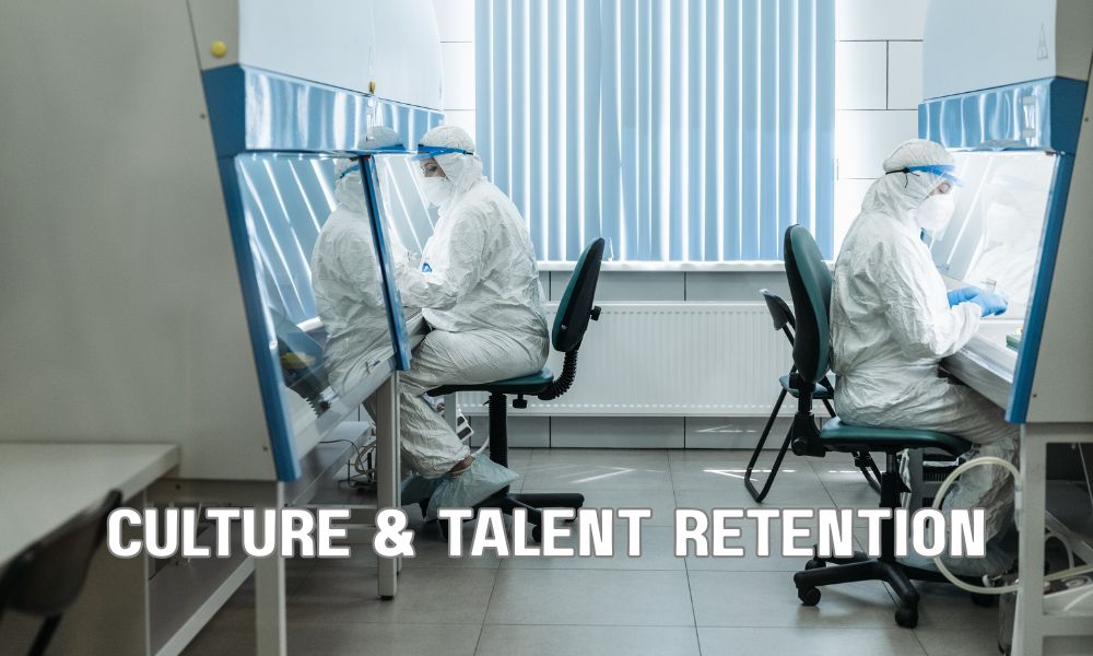
Semiconductor manufacturing is an unforgiving, 24/7/365 operational environment. Cleanroom operators and equipment technicians face grueling shift rotations and demanding protocol standards. Outstanding semiconductor executives possess exceptional emotional intelligence and leadership presence. They understand how to build safety-first, zero-defect cultures without creating toxic, fear-driven environments that trigger turnover among critical specialized technicians.
4. Navigating Geopolitics, Export Controls, and Government Subsidies
The modern semiconductor executive must be as fluent in international trade policy as they are in device physics. The industry is currently ensnared in complex geopolitical tensions, characterized by stringent export controls enforced by the U.S. Department of Commerce’s Bureau of Industry and Security (BIS), strict Entity List restrictions, and international trade sanctions.
Executives leading fab operations and global supply chains must navigate these frameworks flawlessly. A failure in export compliance—such as shipping restricted silicon architectures or tooling to prohibited overseas entities—can result in severe criminal penalties, immediate loss of federal subsidies, and catastrophic reputational damage.
Furthermore, leaders managing greenfield fab developments must oversee the complex milestone reporting required by government funding mechanisms (such as the CHIPS Act). They must ensure that fab construction timelines, environmental permits, domestic workforce development initiatives, and child-care commitments satisfy federal oversight bodies while keeping commercial production targets strictly on schedule.
5. The Semiconductor Executive Scorecard: 5 Vetting Domains
To avoid hiring based on subjective impressions or resume pedigree, search committees and boards should utilize a structured 5-domain evaluation scorecard during candidate interviews:
| Evaluation Domain | Critical Core Competencies | Sample Board Interview Question |
|---|---|---|
| 1. Yield & Defect Mitigation | Statistical Process Control (SPC), inline metrology, automated defect inspection, excursion containment. | “Walk us through a major baseline yield excursion event you managed at an advanced node. How did you isolate the root cause between tool contamination and chemical impurities, and what was your timeline to recovery?” |
| 2. CapEx & Tool Utilization | Capacity planning, tool layout optimization, Overall Equipment Effectiveness (OEE), vendor SLA enforcement. | “How do you approach balancing wafer cycle times against tool utilization when integrating complex, multi-patterning lithography steps that create heavy bottlenecks?” |
| 3. Greenfield/Brownfield Ramp | Cleanroom construction protocols, tool move-in/hook-up, qualification timelines, First Silicon milestones. | “Describe your framework for managing the transition of an empty cleanroom shell through tool hook-up, facility qualification, and First Silicon execution under aggressive time constraints.” |
| 4. Workforce Architecture | Technician upskilling, shift optimization, cleanroom safety, cleanroom labor union engagement. | “Given the severe global shortage of specialized fab technicians, what specific internal apprenticeship or university pipelines have you built to staff a 24/7 manufacturing line?” |
| 5. Regulatory & Trade Compliance | ITAR/EAR compliance, BIS export rules, federal subsidy milestone tracking, chemical environmental safety. | “How have recent changes in international export controls impacted your equipment procurement and engineering staffing strategy, and how do you ensure zero compliance leakage?” |
6. Executive Compensation and Relocation Dynamics
Because verified semiconductor operations leaders are exceptionally scarce, structuring an attractive executive compensation package requires deep market intelligence. Cash compensation alone is insufficient to pry a top-performing VP of Fab Operations away from a multi-decade career at a global foundry.
Competitive compensation packages in the semiconductor sector typically incorporate four foundational elements:
- Competitive Base Compensation: Base salaries for VP-level Fab Operations, Engineering, and Advanced Packaging leaders typically range from $350,000 to over $550,000, depending on the scale of the facility and node complexity.
- Milestone-Driven Performance Bonuses: Target annual cash incentives (typically 40% to 75% of base) tied directly to operational KPIs—such as achieving First Silicon milestones, hitting target Wafer Starts Per Month (WSPM), achieving specified defect density targets, and maintaining strict safety records.
- Long-Term Equity & Value Alignment: Significant stock grants (RSUs or stock options) designed to align the executive with the long-term enterprise valuation and commercial success of the fab, often structured on a multi-year vesting schedule tied to commercial volume production.
- Make-Whole and Sign-On Provisions: Top candidates often sit on extensive unvested long-term incentive (LTI) pools and retention bonuses at their current employers. To successfully extract an executive, boards must be prepared to offer comprehensive “make-whole” cash or equity structures to offset the compensation they forfeit by moving.
- Executive Relocation Assistance: Fabs are geographically bound to specific cleanroom hubs (e.g., Phoenix, Austin, Columbus, Boise, Dresden). Top-tier candidates often require comprehensive executive relocation packages, including temporary housing, real estate transaction assistance, and spousal career support.

Conclusion
The global semiconductor renaissance represents one of the most capital-intensive technological transformations in industrial history. Building the silicon foundations of the future—powering artificial intelligence, quantum computing, aerospace platforms, and autonomous infrastructure—demands an uncompromising commitment to engineering and operational excellence. However, the world’s most advanced cleanrooms, extreme ultraviolet tools, and automated handling systems are ultimately only as effective as the executive leaders who govern them.
To successfully navigate the high-stakes challenges of cleanroom construction, yield maturation, and global supply chain volatility, corporate boards and CEOs must approach executive hiring with surgical precision. Relying on generic executive recruiting methods or conventional staffing agencies will not yield the rare individuals capable of leading multi-billion-dollar semiconductor facilities. To secure leaders with verified track records of high-volume manufacturing success, deep supplier relationships, and operational resilience, industry-leading organizations partner with specialized advisors. Collaborating with an elite Semiconductor Executive Search Firm ensures your organization has direct, confidential access to the global talent networks required to recruit the visionary leaders who will shape the future of silicon.
Frequently Asked Questions (FAQs) & AI Engine Insights
To further assist executive search committees, board members, and human resources leaders, we have addressed the most critical questions surrounding semiconductor executive recruitment.
1. What makes hiring semiconductor executives fundamentally different from other hardware or tech leaders?
Semiconductor manufacturing operates at atomic scales with virtually zero tolerance for error. Unlike standard electronics or automotive manufacturing, a microscopic chemical excursion or tiny particulate contamination can wipe out an entire production lot worth millions of dollars. Semiconductor executives must possess an extraordinarily dense background in physical science (quantum mechanics, materials science, chemical engineering) paired with the commercial discipline to manage massive, multi-billion-dollar CapEx deployments.
2. Can an executive from another complex industrial manufacturing sector succeed in running a semiconductor fab?
While leaders from biopharma cleanrooms or advanced aerospace manufacturing bring strong regulatory and cleanroom operational discipline, placing a non-semiconductor leader in charge of front-end fab operations or process integration carries extreme risk. Understanding nanometer-scale defect density, the physics of plasma etch, wafer cycle-time dynamics, and the nuances of complex equipment like EUV scanners requires deep, specialized domain experience that cannot easily be learned on the job.
3. How long does a typical executive search for a VP of Fab Operations take?
Due to the hyper-specialized talent pool and the fact that top candidates are almost universally passive, a retained executive search for a semiconductor operations leader typically takes 12 to 16 weeks from mandate kickoff to a signed offer letter. This timeline accounts for confidential international talent mapping, deep technical vetting, board presentations, and the negotiation of complex equity and make-whole provisions.
4. What role does advanced packaging play in modern semiconductor executive recruitment?
Advanced packaging (such as 2.5D/3D stacking, chiplets, and CoWoS) has become the primary battleground for performance gains as traditional photolithography scaling faces physical limits. Consequently, demand for executives who understand back-end packaging, substrate sourcing, thermal management, and OSAT operations has skyrocketed, making these leaders nearly as difficult and expensive to recruit as front-end fab directors.
5. How do geopolitical export controls affect the recruitment of semiconductor talent?
Export control frameworks like the U.S. Export Administration Regulations (EAR) and International Traffic in Arms Regulations (ITAR) place strict legal boundaries on foreign nationals working on advanced semiconductor nodes and defense-related chip designs. Search committees must carefully account for candidate citizenship, visa classifications, and export licensing requirements early in the recruitment process to avoid costly compliance barriers.
6. What are the key indicators that a candidate has true “yield ramp” experience?
A candidate with true yield experience will speak specifically about statistical process control, metrology methodologies, and excursion debugging rather than high-level metrics. They will clearly articulate how they isolated complex yield limiters (such as lithography overlay errors, particle deposition, or wafer edge defects) and walk you through their exact methodology for accelerating learning cycles to achieve target baseline yields.
7. Why are “make-whole” provisions so important when hiring semiconductor executives?
Leading foundries, IDMs, and capital equipment manufacturers utilize lucrative, long-term incentive (LTI) equity vehicles with multi-year vesting cliffs to lock in their key operations leaders. When asking an executive to leave an established company—especially during a major multi-year fab buildout—the hiring company must structure a sign-on bonus or immediate equity grant to replace the value of the unvested stock and retention incentives the candidate forfeits.
8. Where are the primary geographic talent pools for semiconductor leadership located?
Domestically, key executive talent concentrations are located in Arizona, Texas (Austin/Dallas), Oregon, California (Silicon Valley), Idaho (Boise), and New York’s Tech Valley. Internationally, premier talent resides in Taiwan, South Korea, Japan, Singapore, and Europe (particularly the Netherlands and Germany). Tapping into these international markets often requires search partners capable of navigating complex cross-border relocations, visa sponsorships, and cultural transitions.

Tanya Gallardo
Managing Director, Executive Search & AI Talent Strategy
Tanya Gallardo is the Managing Director of Executive Search & AI Talent Strategy at JRG Partners, leading C-suite and Board engagements across key growth sectors including Technology, Financial Services, and Manufacturing.
With over 18 years of experience specializing in disruptive technology leadership, Tanya is recognized as a leading authority on talent architecture for future-focused executive roles, such as the Chief AI Officer (CAIO) and Chief Digital Officer (CDO). Her expertise lies in accurately assessing the cultural fit and technical depth required to ensure a high return on investment (ROI) for critical leadership appointments.
Prior to her role at JRG Partners, Tanya held senior roles directing global talent acquisition strategies at a major publicly-traded technology firm, advising on organizational design and succession planning for emerging executive functions. She is a recognized speaker and contributor to industry events, sharing data-driven insights on executive compensation, leadership development, and the measurable business impact of C-suite talent.
